Lab 7: AES-128 Hardware Accelerator & SPI MCU Link
Introduction
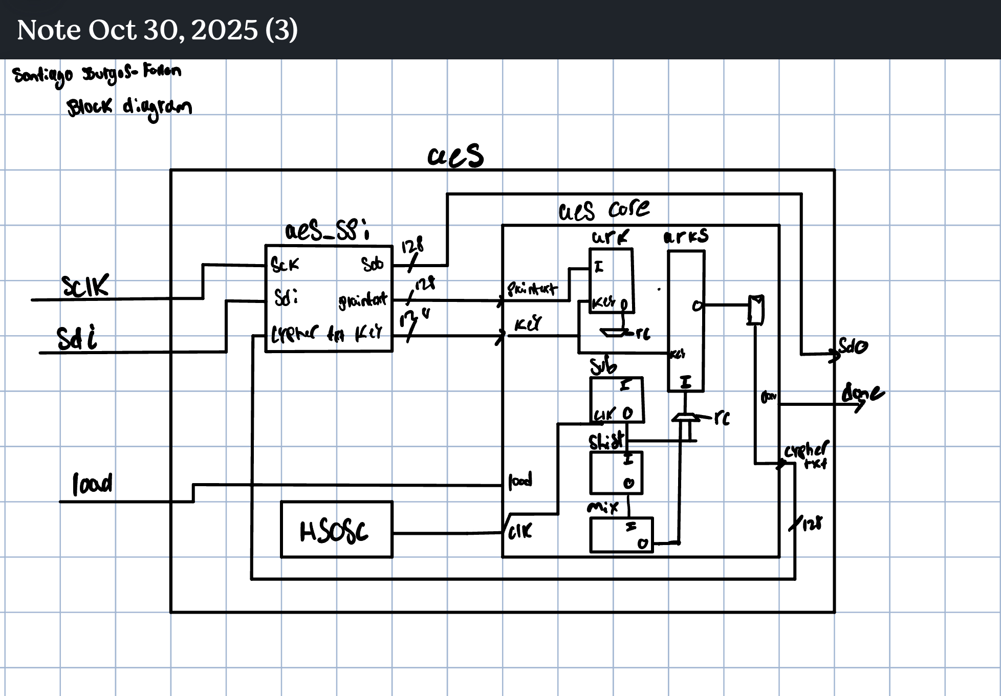
In this lab I implemented a 128-bit AES encryption accelerator in SystemVerilog and wrapped it with a simple SPI shift interface so an MCU can send a key and plaintext and read back the ciphertext. The AES core is an iterative, multi-cycle design (1 round per few cycles) sized to the FPGA’s resources. I verified function first in simulation (core TB, then SPI TB), then used a logic analyzer to confirm timing and bit ordering on the hardware link.
Learning outcomes: specification-driven design, datapath + controller partitioning, MCU↔︎FPGA interface timing, structured debug with simulation + LA, and a taste of hardware acceleration.
System Overview
Top-level flow. MCU →(SPI: 256 SCK in)→ FPGA (aes_spi) → aes_core → ciphertext latched →(SPI: 128 SCK out)→ MCU, which compares against a known test vector.
AES mode. AES-128, Nr = 10 rounds (Nk = 4, Nb = 4). The round sequence is:
- Initial AddRoundKey
- Rounds 1–9: SubBytes → ShiftRows → MixColumns → AddRoundKey
- Round 10: SubBytes → ShiftRows → AddRoundKey (no MixColumns)
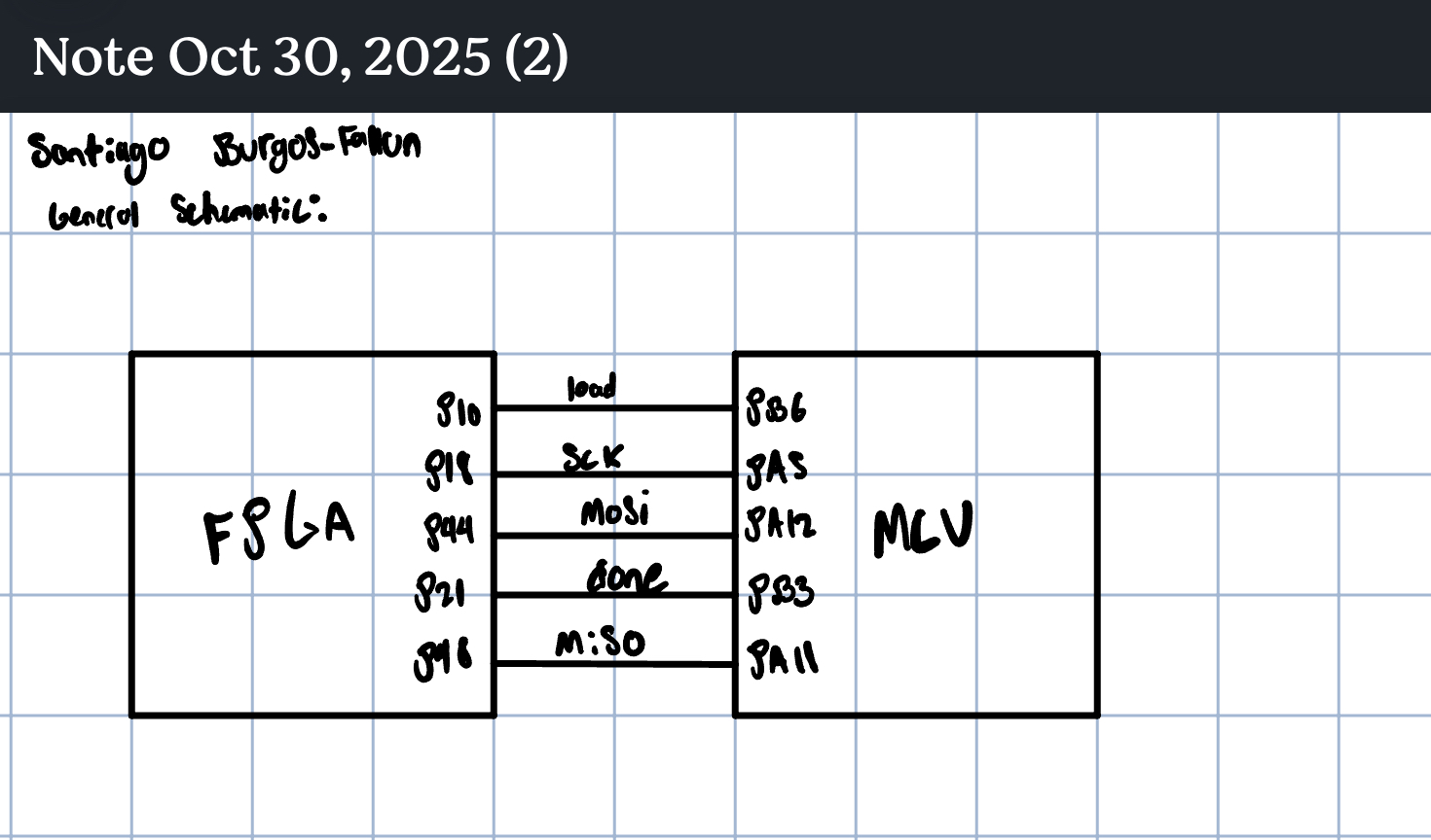
SPI Interface (FPGA side)
- Mode CPOL=0/CPHA=0: sample
sdion posedge SCK; updatesdoon negedge SCK. - Shift-in phase (256 edges):
{plaintext, key}MSB-first. - Compute phase:
loaddeasserted; core runs ~11 fabric clocks and raisesdone. - Shift-out phase (128 edges): cipher MSB-first; the first MSB is driven as soon as
donerises (before next SCK edge), thensdoupdates on negedges.
Design Approach
Datapath
- State register (128b) holds the current AES state.
- RoundKey register (128b) holds the active round key.
- SubBytes: 16×
sbox_sync(1-cycle, uses BRAM;sbox.txtROM init). - ShiftRows: hard-wired byte permutes.
- MixColumns: 4× column units with GF(2^8) multiply-by-x helper (
galoismultwith poly0x1B). - AddRoundKey: 4× 32-bit XORs.
Controller (FSM)
States (conceptually):
- IDLE — wait for
load; stage plaintext/key for initial ARK. - INIT_ARK — compute
state = plaintext ^ key. - ROUND_PREP — present
stateto SubBytes; keyexp sees{round, rk}. - SUB_ISSUE / SUB_CAPTURE — burn 1 cycle for
sbox_sync, latchSubBytes. - SR_STAGE — apply ShiftRows.
- MC_STAGE — apply MixColumns (skip when
round==10). - ARK_STAGE / ARK_FINAL — XOR with next round key; increment round; on final, latch
cyphertextand assertdone. - FINISH — hold
donehigh until nextload.
Key Expansion (AES-128)
- Implements RotWord → SubWord → XOR with Rcon on the last word, then chained XORs to form the next 128-bit round key.
- Rcon sequence uses
{0x01, 0x02, 0x04, …, 0x1B, 0x36}for rounds 1..10. - SubWord uses the same sbox_sync (1-cycle).
Implementation Notes
- The iterative core fits comfortably; the S-box is the dominant area (maps to BRAM/LUT RAM depending on tool inference).
- Because sbox_sync is synchronous, I inserted an explicit one-cycle gap between presenting bytes and capturing the substituted result.
- The final round bypasses MixColumns via a small mux on the ARK input.
- The SPI module double-buffers the outbound ciphertext so
sdois valid immediately ondoneand then continues shifting on SCK negedges.
Test Plan
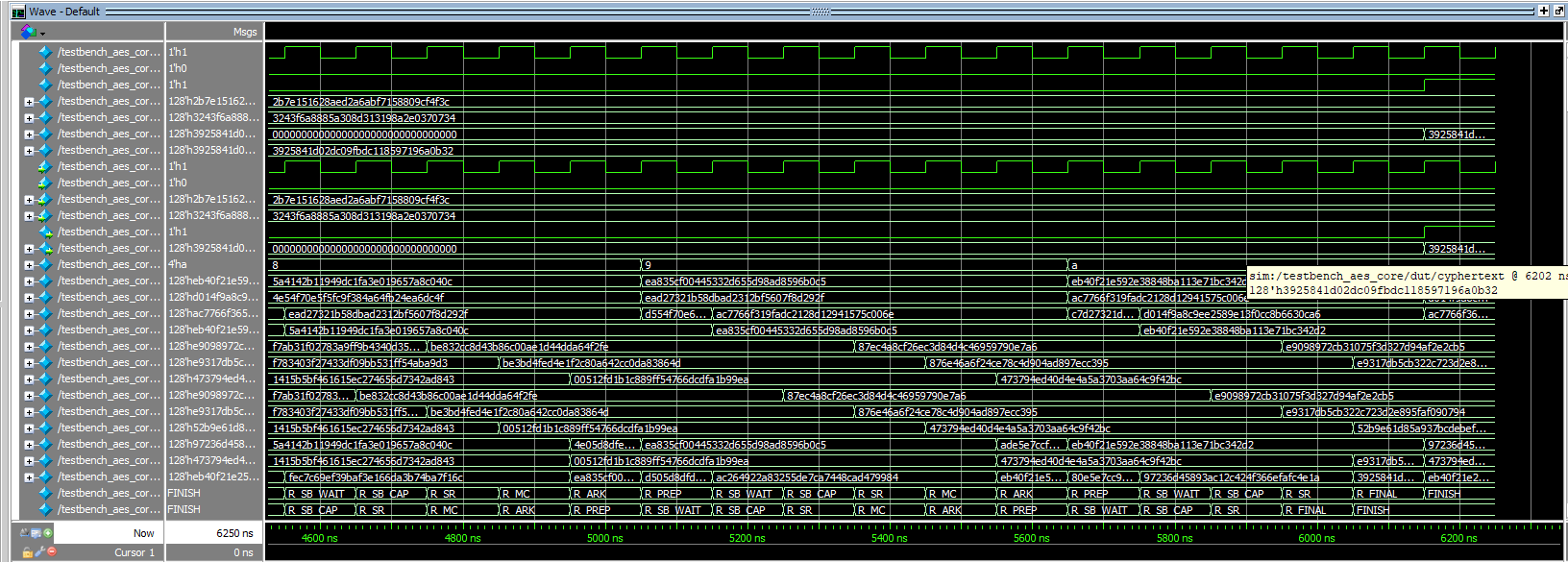
Functional Vectors (Core TB)
NIST AES-128 example (Appendix A/B):
key = 2b7e151628aed2a6abf7158809cf4f3cplaintext = 3243f6a8885a308d313198a2e0370734- Expected
ciphertext = 3925841d02dc09fbdc118597196a0b32
The core TB drives
load, clocks through 10 rounds, and checksdoneand the final value.
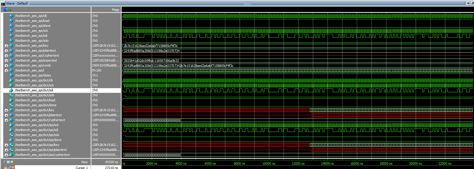
End-to-End SPI (SPI TB)
- Shifts
{plaintext, key}MSB-first onsdiwith 256 posedges. - Deasserts
loadand waits fordone. - Samples
sdoon posedge SCK while I update it on negedge (128 cycles). - Compares the assembled 128-bit value with the golden.
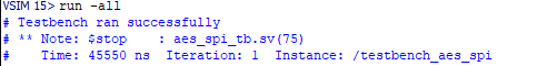
- On success, the TB prints “Testbench ran successfully” and calls
$stopto allow wave inspection.
MCU ↔︎ FPGA Interface
The provided
lab7.cdrives the SPI transaction and compares the ciphertext locally. No changes needed as long as:- CPOL/CPHA = 0/0 (match FPGA).
- NSS/CE held active during each continuous shift window.
- Bit order MSB-first.
On success, the MCU prints a pass banner and can toggle a status LED.
Results
- Core TB: passes the NIST vector.
- SPI TB: passes end-to-end; ciphertext matches.
Time Spent
~20 hours .
Known Limitations / Future Work
- Current core is encrypt-only; no decryption path.
- One round per several cycles; could pipeline rounds for higher throughput (at area cost).
- Add AXI-lite or memory-mapped interface for queued requests.
- Parameterize for AES-192/256 key sizes.
Schematic standards: labeled pins/parts/values, junction dots, left-to-right flow, neat layout, title block. HDL standards: one module/file, descriptive names, comments, clear hierarchy, individual module TBs, include TB outputs in report.
AI Prototype
Prototype A — With Spec (FIPS-197 available)
Prompt. “Write SystemVerilog HDL to implement the KeyExpansion logic described in the FIPS-197 uploaded document. The module should be purely combinational, using the previous key and current round number to calculate the next key. Assume other required modules (SubWord and RotWord) are already implemented.”
Outcome (what happened). The LLM produced a clean combinational keyexpansion with:
- Correct Rcon mapping for rounds 1..10.
RotWordthenSubWordonw3, XOR chainw0'..w3'.- Proper port widths and MSB-first word ordering.
Analysis. It synthesized immediately. Because my in-lab design uses synchronous SubWord (via sbox_sync), I swapped the prototype’s pure-comb SubWord call for my existing registered version and inserted one holding cycle in the controller. The generated structure matched FIPS-197, so functional results were identical.
Prototype B — Without Spec (No “AES” Mention)
Prompt. (Rephrased, no “AES” terms; uses the provided abstract pseudocode with module1, module2, Rcon and loop unrolling instructions.)
Outcome (what happened). The LLM generated a module that:
- Preserved the word-wise recurrence and XOR chain.
- Exposed a param for Nk and Nr, but mis-handled
Rconfori/Nk ≥ 9(missed0x1B→0x36step). - Treated
module1/module2as black-box instances correctly, but defaulted them to combinational timing.
Analysis. Functionally close but not spec-exact (Rcon corner), which is expected without domain context. After I fixed the Rcon table and aligned timing to my synchronous SubWord, it matched Prototype A. Takeaway: LLMs can mirror control/data recurrences from pseudocode well, but spec-driven constants (like Rcon sequences) still need expert review.