Lab 2: Multiplexed 7-Segment Display
Introduction
In this lab I implemented time-multiplexing to drive a dual common‑anode seven‑segment display using a single hex→segments decoder module. Two 4‑bit nibbles (from DIP switches) are alternately presented to the decoder; high‑side PNP transistors enable exactly one digit at a time. I also displayed the 5‑bit sum of the two hexadecimal inputs on five LEDs and verified safe currents per the iCE40‑UP5K datasheet (§4.17). Designs were simulated in QuestaSim and synthesized in Lattice Radiant.
Design & Testing Methodology
Architecture

top).
- Clocking. The internal HF oscillator (HSOSC) runs at 6 MHz (
CLKHF_DIV=2'b11).
- Multiplexer/Scan.
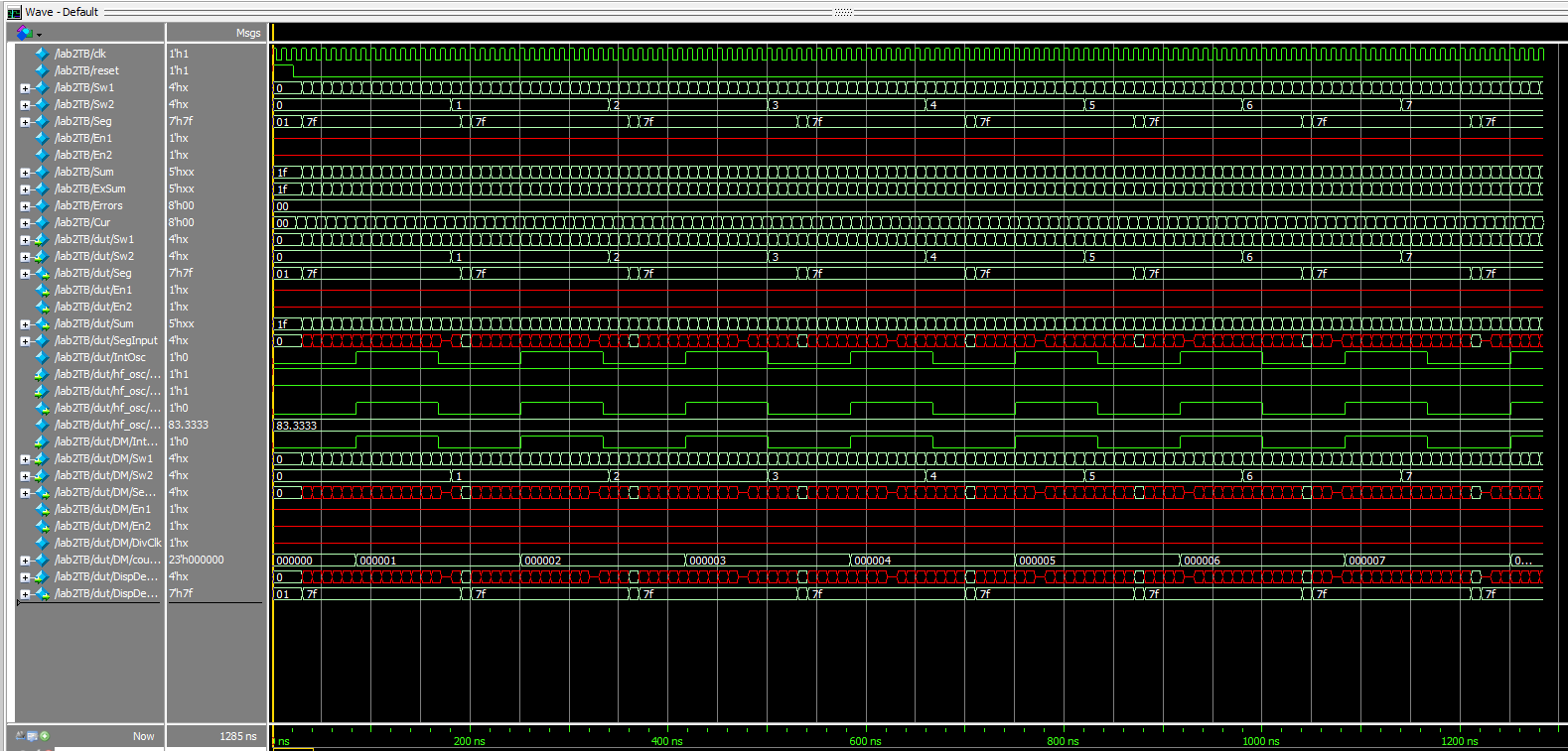
Dmuxdivides the 6 MHz clock to a scan clockDivClk, selects which nibble feeds the decoder, and asserts the corresponding digit enable (En1,En2).
- Decoder.
SevenSegis a combinational hex→segments decoder with active‑LOW outputs for a common‑anode display (Seg[6:0], whereSeg[0]=A … Seg[6]=G).
- Top‑level.
topwires the pieces together and computes the 5‑bit sum onSum[4:0](LEDs are active‑LOW on our board, so the sum is inverted).
Multiplex timing
With HSOSC at 6 MHz and terminal count N, Dmux toggles DivClk every N cycles; the scan frequency is:
\[ f_{\text{scan}}=\frac{f_{\text{clk}}}{2N}. \]
In my current code \(N=60{,}000\), so
\[ f_{\text{scan}}=\frac{6\,\mathrm{MHz}}{2\cdot 60{,}000}\approx \mathbf{50\ \mathrm{Hz}}. \]
HDL overview (key excerpts)
top.sv- HSOSC at 6 MHz, instantiates
DmuxandSevenSeg, drivesSum = ~(Sw1 + Sw2).
- HSOSC at 6 MHz, instantiates
Dmux.svSegInput = (DivClk) ? Sw1 : Sw2;
En1 = ~DivClk; En2 = DivClk;
- Counter toggles
DivClkat the chosen scan rate.
SevenSeg.sv- 16‑entry
caseproducing active‑LOW segment patterns for 0x0–0xF (e.g.,4'b1001 /*9*/ → Seg=7'b0001100).
- 16‑entry
Unit tests (simulation)
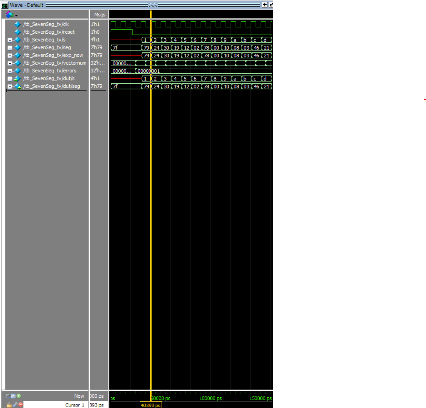
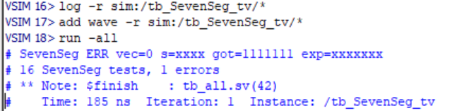
SevenSeg_tb.sv(self‑checking): sweeps all 16 hex values and comparesSegto expected patterns.
top_tb.sv: iteratesSw1, Sw2over 0x00–0xFF and checksSum == ~(Sw1 + Sw2)and basic enable/segment sanity during scanning.
Dmux_tb.sv: spot‑checks scan duty and selection timing.
Electrical Design: red LED current calculations
This display is common‑anode. Each segment has its own resistor and is sunk by an FPGA pin when ON (segment output = 0). The anode of the active digit is driven high via a PNP (2N3906). 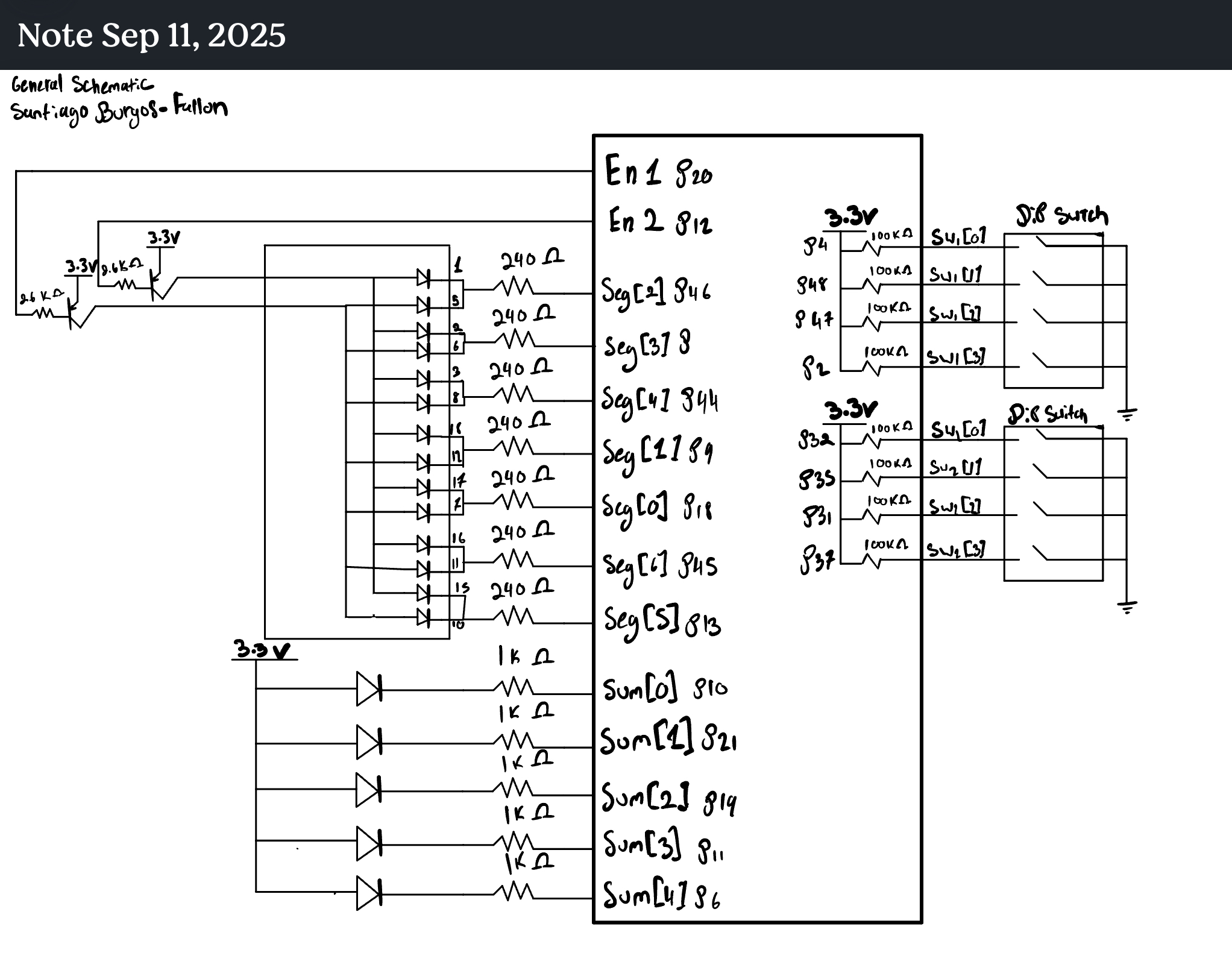
Segment resistor (per segment, \(\mathbf{R} = 240\,\Omega\); common-anode, FPGA sinks)
With a PNP digit switch, the active digit’s anode is approximately \(3.3 - V_{\mathrm{CE,sat}}\). The cathode path includes the LED and the FPGA’s \(V_{\mathrm{OL}}\).
\[ V_{\mathrm{R}} = (3.3 - V_{\mathrm{CE,sat}}) - V_{\mathrm{F}} - V_{\mathrm{OL}}, \qquad I_{\mathrm{seg}} = \frac{V_{\mathrm{R}}}{R_{\mathrm{seg}}}. \]
Use conservative bounds \(V_{\mathrm{CE,sat}} \approx 0.25\,\mathrm{V}\) (2N3906) and Table 4.13 limits for \(V_{\mathrm{OL}}\).
Typical case (\(V_{\mathrm{F}} \approx 1.8\,\mathrm{V}, V_{\mathrm{OL}} \approx 0.2\,\mathrm{V}\)): \[ V_{\mathrm{R}} = 3.3 - 0.25 - 1.8 - 0.2 = 1.05\,\mathrm{V}, \qquad I_{\mathrm{seg}} = \frac{1.05}{240} \approx 4.38\,\mathrm{mA}. \]
Conservative case (\(V_{\mathrm{F}} \approx 2.0\,\mathrm{V}, V_{\mathrm{OL}} \approx 0.4\,\mathrm{V}\)): \[ V_{\mathrm{R}} = 3.3 - 0.25 - 2.0 - 0.4 = 0.65\,\mathrm{V}, \qquad I_{\mathrm{seg}} = \frac{0.65}{240} \approx 2.71\,\mathrm{mA}. \]
Because the display is multiplexed at ≈50 % duty, the average segment current is \[I_{\mathrm{seg,avg}} \approx 0.5 \cdot I_{\mathrm{seg}}\] ≈2.19 mA typical, ≈1.35 mA conservative.
Solid stand-alone red LEDs (\(\mathbf{R} = 1\,\mathrm{k\Omega}\), FPGA sinks, no PNP)
Here the resistor sees \(V_{\mathrm{R}} = 3.3 - V_{\mathrm{F}} - V_{\mathrm{OL}}\).
Typical (\(V_{\mathrm{F}} \approx 1.8\,\mathrm{V}, V_{\mathrm{OL}} \approx 0.2\,\mathrm{V}\)): \[I = \frac{3.3 - 1.8 - 0.2}{1000} = \frac{1.3}{1000} \approx 1.30\,\mathrm{mA}.\]
Conservative (\(V_{\mathrm{OL}} \approx 0.4\,\mathrm{V}\)): \[I = \frac{3.3 - 1.8 - 0.4}{1000} = \frac{1.1}{1000} \approx 1.10\,\mathrm{mA}.\]
PNP anode driver (per digit, \(\mathbf{R}_{\mathrm{B}} = 1\,\mathrm{k\Omega}\))
Worst-case segment load when displaying “8”: \[I_{\mathrm{C}} \approx 7 \cdot I_{\mathrm{seg}}.\]
Base-resistor drop when ON: \[V_{\mathrm{RB}} \approx V_{\mathrm{E}} - V_{\mathrm{BE,sat}} - V_{\mathrm{OL}}.\]
With \(V_{\mathrm{BE,sat}} \approx 0.65\text{–}0.85\,\mathrm{V}\) and \(V_{\mathrm{OL}} \approx 0.2\text{–}0.4\,\mathrm{V}\), \[V_{\mathrm{RB}} \approx 3.3 - (0.65\text{–}0.85) - (0.2\text{–}0.4) \approx 2.45\text{–}2.05\,\mathrm{V}.\]
For \(R_{\mathrm{B}} = 1\,\mathrm{k\Omega}\), \[I_{\mathrm{B}} \approx \frac{V_{\mathrm{RB}}}{R_{\mathrm{B}}} \approx 2.05\text{–}2.45\,\mathrm{mA}.\]
Forced-beta check \(\beta_{\mathrm{forced}} = I_{\mathrm{C}} / I_{\mathrm{B}}\):
Typical brightness (\(I_{\mathrm{seg}} \approx 4.38\,\mathrm{mA}\)): \(I_{\mathrm{C}} \approx 30.6\,\mathrm{mA}\), \(\beta_{\mathrm{forced}} \approx 12.5\text{–}15\).
Conservative brightness (\(I_{\mathrm{seg}} \approx 2.71\,\mathrm{mA}\)): \(I_{\mathrm{C}} \approx 19.0\,\mathrm{mA}\), \(\beta_{\mathrm{forced}} \approx 7.8\text{–}9.3\).
These values are suitable for saturating a 2N3906 in this current range.
Technical Documentation
- Code directory (this lab):
top.sv— top level (HSOSC @ 6 MHz, Dmux, SevenSeg, Sum LEDs)Dmux.sv— divider + input select + digit enablesSevenSeg.sv— hex→7‑segment decoder (active‑LOW)*_tb.sv— basic testbenches (SevenSeg_tb.sv,Dmux_tb.sv,top_tb.sv)
- Tools: Radiant (synthesis, constraints, Netlist Analyzer), QuestaSim Lattice Edition (simulation).
Notes that matter for this lab
- Active‑LOW segments. Common‑anode means driving a
0turns a segment ON. Keep all case patterns consistent with this polarity. - One decoder only. Both digits share the same decoder → time‑multiplex inputs and enables.
- Brightness uniformity. Identical per‑segment resistors and a fixed 50% duty for each digit keep perceived brightness similar across numbers.
- Scan rate. If you observe flicker or “ghosting,” increase \(f_{\text{scan}}\) (reduce
N).
Results & Discussion
- The decoder produced the correct segment patterns for 0x0–0xF in simulation and on the physical board. The summing LED’s also followed the expected behavior.
- At (N=60,000) (≈50 Hz scan), both digits are readable, with no visible flicker present.
- The 5‑bit
SumLEDs matchedSw1 + Sw2for all 256 input pairs in the top‑level test.
Conclusion
I met the Lab 2 requirements: a single seven‑segment decoder time‑multiplexed across two digits, the sum on five LEDs, and current‑safe driving using PNP anode switches with per‑segment resistors. The design is modular (Dmux, SevenSeg, top) and synthesizes cleanly.
Time spent: (8) hours.
AI Implementation
Prompt used
Write SystemVerilog HDL to time multiplex a single seven segment decoder (that decodes from four bits to a common anode seven segment display) to decode two sets of input bits and drive two sets of seven output bits. Use the seven segment decoder and oscillator provided in the attached files.
What the LLM produced
- Good ideas it used
- Kept one hex→7-segment decoder and time-multiplexed the inputs (correct per spec).
- Added a parameterized scan divider with
$clog2sizing and a cleanalways_ffcounter. - Split the design into clear modules: a scan/mux block (selects nibble + digit enables) and the existing decoder.
- Used
always_combfor pure combinational logic and documented active-LOW segment polarity (common-anode). - Suggested a sim mode with a tiny divider under
ifndef SYNTHESISto speed testbenches.
- Gaps I had to fix
- The first draft instantiated the decoder twice (one per digit). I rewired to feed a single decoder with the selected nibble.
- Digit enable polarity was backward for a PNP high-side scheme; I inverted the enables so only one anode is ON at a time.
Quality rating (and why)
- Rating: B+
- Why: Architecture and modularity were solid, scan logic was close to correct, and it respected the “single decoder” objective after edits. Minor polarity mistakes and a comment/math mismatch kept it from an A.
Did it synthesize first time?
- Not exactly. With the provided oscillator and decoder, it built after two small fixes:
- Removed the duplicate decoder instance and fed the single instance from the scan mux.
- Flipped digit-enable polarity to match the common-anode via PNP wiring.
- Removed the duplicate decoder instance and fed the single instance from the scan mux.
What I’d do differently next time with an LLM
- Pin down polarity & wiring in the prompt: “common-anode, active-LOW segments, PNP digit enables, single decoder” to avoid the duplicate-decoder and enable-polarity missteps.
- Specify the exact primitives up front: “use the provided HSOSC and SegDisp modules by name” to prevent library/primitive swaps.